Twisted science
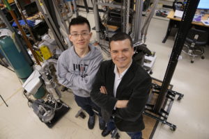
Pablo Jarillo-Herrero (right), Cecil and Ida Green Professor of Physics at MIT, was honored with Physics World’s 2018 Breakthrough of the Year for his group’s discovery of magic-angle graphene, a promising technique for adjusting the electronic properties of graphene. Graduate student Yuan Cao (left) was a lead researcher in the work. Photo: Melanie Gonick
Since my childhood, I have been intrigued by how everything works in nature. I’ve always asked myself, “Why does this have to work this way?” This curiosity was what encouraged me to choose a slightly different path than most other teenagers in China, enrolling in a special class for young students at the University of Science and Technology of China when I was 14. The year I entered college, 2010, was also the year when graphene — the magic one-atom-thick material consisting purely of carbon — won its discoverer the Nobel Prize in physics, and became the first big scientific breakthrough I became aware of. That same year, theoretical physicists predicted that a precise twisting of graphene might confer properties unlike anything the physics world had seen before.
In a lab class in my third year in college, I was given the freedom to design my own experiment. I fabricated a graphene-silicon photodetector with a few of my friends. When excited by photons from a light source, the electrons in the graphene at a graphene-silicon junction can jump into the silicon and produce an electric current, allowing us to detect the light. Although the complexity of the device is nowhere comparable to my current research, I was amazed by the beauty of this material: a single-layer of carbon atoms can produce an electronic signal whenever I point a laser pointer at it! From that time on, I decided I wished to know more about this almost magic-like material of graphene, and that’s why I chose to join Cecil and Ida Green Professor of Physics Pablo Jarillo-Herrero’s lab at MIT.
As a condensed-matter physics lab, we mainly study the fundamental question of how electrons in a twodimensional material like graphene move and how we can tweak the materials to achieve the electronic properties we want, from a semiconductor that stops the electrons from flowing altogether, to a superconductor where electrons can flow freely without any resistance. My project over the past few years has focused on the electronic properties of a twisted structure. The idea is quite simple: I take two sheets of graphene and stack them together with a twist so that the carbon atoms don’t align with each other. Despite the simplicity, it turns out that this crucial twist brings us unprecedented richness in the physical phenomena in this material.
Give it at twist
Physicists had known for a long time that the electrons in graphene move in a “relativistic” way — that is, like light, they move at a constant speed, which is about 1/300 of the real speed of light. This property of these electrons, also known as Dirac electrons, is the fundamental reason behind the peculiar properties of graphene and also why graphene could potentially be revolutionary for future electronic devices.
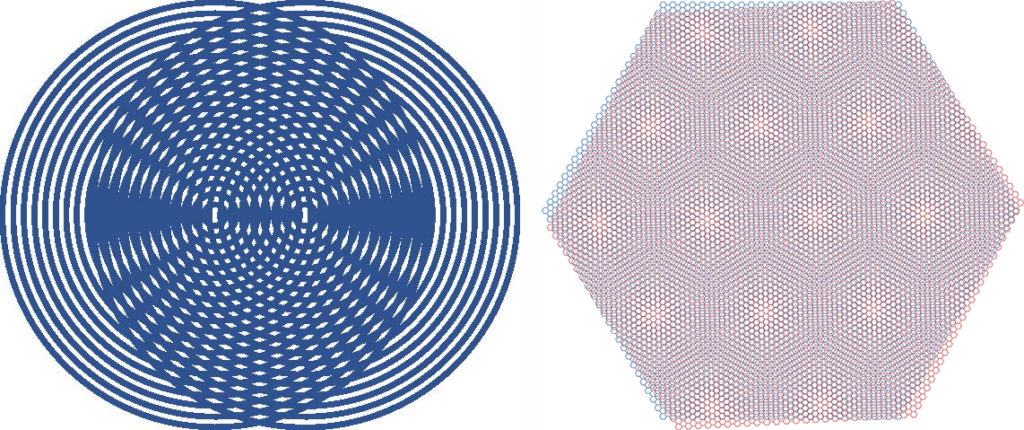
The idea of twisting graphene comes from a prediction made by theoretical physicists at University of Texas at Austin, back in 2010. According to their hypothesis, when one puts one layer of graphene on another with a magic twisting angle of approximately 1.1 degrees, the electrons behave in a vastly different manner; their speed drops to zero, meaning they are almost completely stuck in space, although they can move in their individual layers! This unexpected phenomena is a result of the moiré pattern that forms between the rotated graphene lattices.
In solid-state physics, the situation in which the electrons are seemingly stuck inside a lattice is called a flat-band condition. Electrons in this state are known to behave strangely, since they are stuck in place and forced to strongly interact with other electrons nearby. One famous example of such a state is copper-oxide compounds, which are known for being superconducting at very “high” temperatures above absolute zero Kelvin (which is still hundreds of degrees lower than room temperature at around 300 Kelvin). The understanding of the behavior of copper-oxides has been one of the biggest challenges in the condensed-matter physics community for more than three decades. I thought that if we could realize a flat-band condition and maybe also superconductivity in a graphene system, it would probably be tremendously helpful for understanding the physics behind the high-temperature superconductivity in copper-oxide, because graphene is a much simpler material (only one element compared to four in copper-oxides).
Tear and stack
As experimentalists, we don’t only think about the question of how electrons move in graphene and other materials, such as copper-oxides. Rather, we need to find suitable ways of realizing these devices in our laboratories and testing our hypotheses by measuring the electrical
properties in a low-temperature apparatus (in fact colder than anywhere in our solar system!) called the cryostat. In our lab, the typical size of the graphene devices that we fabricate on a silicon chip is usually on the order of several to tens of micrometers — about 1/100 to 1/20 of the thickness of human hair. Therefore, all our experiments require steady hands and delicate instruments to precisely stack the required materials together to achieve the configurations we desire to study. The key instrument that we used to achieve this high-precision procedure is called a transfer setup, which is essentially a miniature mechanical arm that we can manipulate in submicron resolutions under a microscope.
The main difficulty in obtaining the twisted graphene structure is to know how to accurately set the twist angle between the graphene layers, as even a mere 0.2 degree difference from the magic angle will completely destroy the phenomena we seek. The approach I took to solve this issue was to tear one piece of large graphene into two, and then stack these two pieces together again, so that they were guaranteed to maintain the same crystal orientation. This is easier said than done; it took me almost two years after I joined the Jarillo-Herrero group to improve the transfer setup and perfect the recipes for this tear-and-stack method.
The effort did pay dividends, as I could then routinely obtain twisted graphene structures with twist angles within 0.1 degrees of what I wanted. With this method, we were one of the first research groups to be able to test the theories on twisted graphene structures. In a paper that I published in Physical Review Letters in 2016, I demonstrated that at angles larger than the magic angle, the properties of twisted bilayer graphene essentially behave exactly like what the band theory of solids would predict.
Proof of principle
The big moment came in the summer of 2017, when I finally obtained two working devices with twist angles near the magic angle. It turned out that the magic-angle twisted bilayer graphene is actually a superconductor in the right conditions — that is, it possess absolutely zero resistance when an electrical current flows through it! Even more interestingly, the superconductivity in the twisted graphene is much like what has been seen in copper-oxide compounds, so we can, in principle, test many hypotheses once proposed for copper-oxide in this much more elegant system.
This proof of principle is why, although the superconducting temperature is not that impressive (the “highest” temperature we’ve achieved so far is about three Kelvin), our Nature paper published in March 2018 received great attention from the entire physics community, and has been cited by other researchers almost a thousand times in less than two years. The physics community has realized that a lot of cool stuff can be squeezed out of two dimensional materials, not limited to graphene, by tuning this “knob” — the twist angle that had been largely overlooked.
As always, with new understanding there is more that we don’t understand. The puzzles about the superconductivity in twisted graphene is far from completely solved. As the twist angle turned out to be so important in these stacked structures, naturally another future direction is to extend the same technology to other two-dimensional materials, such as transitional metal dichalcogenides that are a class of semiconductor materials that can also be thinned down to atomic thickness, just like graphene.
One key question is whether the superconducting state is unconventional as opposed to classic superconductors, such as aluminum and lead, which have been thoroughly studied in the past. In the future, we want to design experiments and devices to test the symmetry of the superconducting state, which would help us differentiate unconventional versus conventional superconductivity. As for myself, I would like to continue exploring the intriguing properties of two-dimensional conductors and superconductors, maybe using slightly different approaches — such as optical microscopy and scanning probe techniques in the future.
Yuan Cao is a sixth year PhD student in the Jarillo-Herrero group in the Department of Electrical Engineering and Computer Science. In 2018, Jarillo-Herrero’s and Cao’s discovery was named the Breakthrough of the Year by Physics World.
This article appeared in the Winter 2020 issue of Science@MIT